FPGA-based Sudoku game
Simulation, testing, and PCB design of Sudoku game with an Intel FPGA controller coded in VHDL

Introduction
So why did I decide to make an FPGA-based Sudoku game? Well, for starters, I’ve been a casual Sudoku player since high school. After spending the holidays with a close friend and her family, during which we played through a bunch of Sudoku puzzles in magazines and booklets, it dawned on me that an electronic version of the classic game could offer a lot of flexibility and enjoyment. Plus, I figured that it would be fun to create!
During this time, I had a strong desire to learn about FPGAs. I’m a strong opponent of “learning by doing”, so I sought to create a Sudoku game based upon an Intel MAX 10 FPGA. I was excited to take on a challenging yet rewarding project, incorporating analog and digital skills and techniques.
Thanks to the project, I further developed my embedded and digital design skillset through practical application and problem solving. Furthermore, I learned how to code in VHDL, gained experience with FSMs as controllers with datapath, and worked with a large number of digital logic entities, (registers, counters, encoders, RAM/ROM, etc.). I found solutions for keyboard input and LED matrix multiplexing which I simulated and tested. On the hardware side, I designed a PCB for the system using the Altium Designer software. Finally, this was my first project using version control (Git) for documentation and for easier iteration during the design phase.
Concept
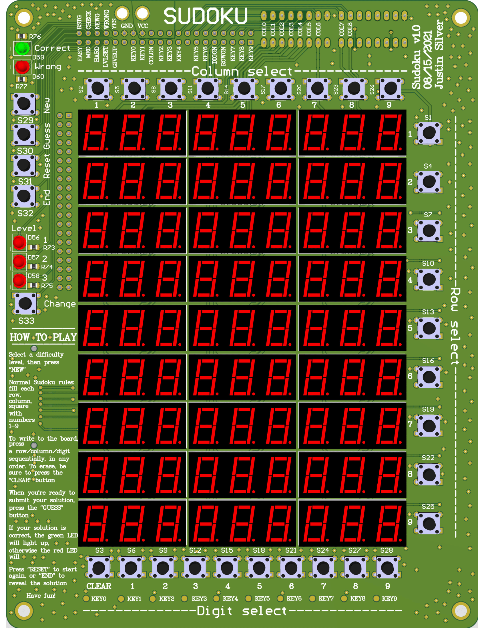
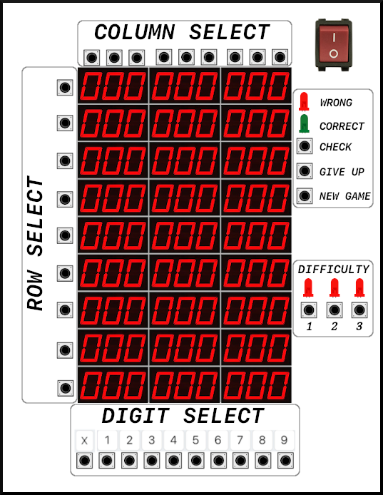
My vision involved a tablet-like device with a 9x9 LED digit display. Around the display, 9 ROW buttons and 9 COLUMN buttons (corresponding to each row and column of the LED digit matrix). On the bottom, 10 buttons corresponding to 9 numerical digits (1, 2, 3… etc.) and 1 clear button. On the side, 3 buttons for submitting a solution, displaying the correct solution, and starting a new game (a later version would include a difficulty setting). Finally, a green and red LED indicates if the player’s proposed solution was correct. This design is summarized in the following photo:
To place a number onto the board, the player selects a row position by pressing one of the ROW buttons, then selects a column position by pressing one of the COLUMN buttons. He or she then chooses a number from the digit keyboard to fill the specified position on the LED matrix. The order doesn’t matter, (as we will see later) so long as the user inputs the 3 within a certain timeframe.
The player continues like this, working through the Sudoku puzzle until completion. The “CHECK” button is then pressed and the device indicates success or not with the LED indicators. The player can then either continue the game, end it by displaying the correct response, or begin a new one.
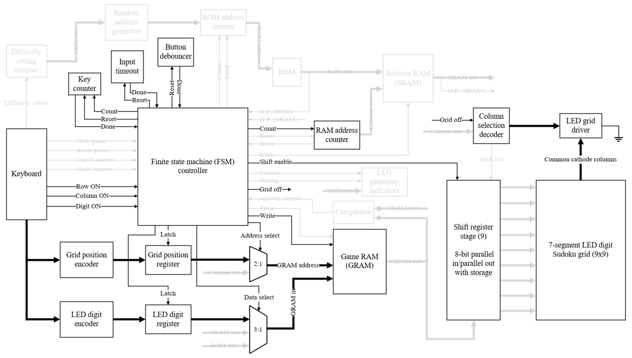
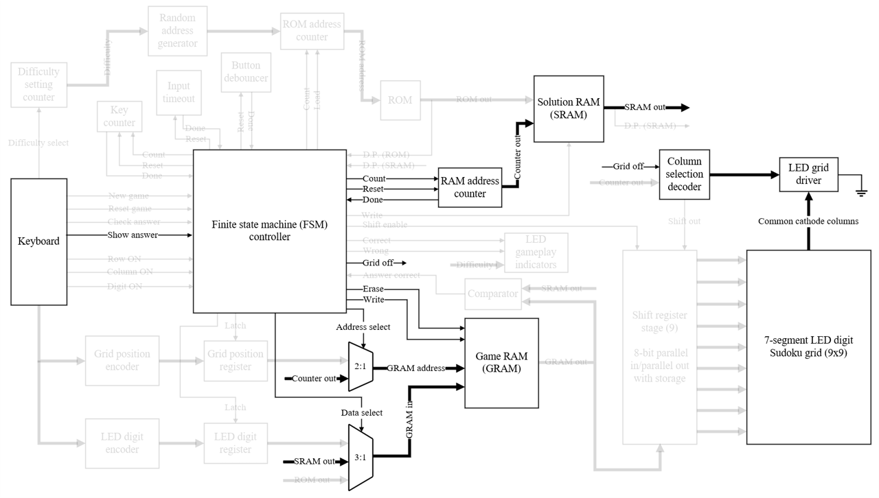
Block diagram
The block diagram can be broken into 4 distinct parts, and the different datapaths highlighted according to the various system states:
- User input
- FPGA processing
- LED output driver
- 7-segment LED digit matrix
Full block diagram
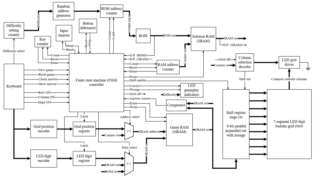
No input detected
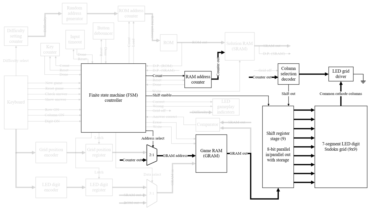
When no input is detected, the system is in its natural state. The RAM address counter continuously cycles through GRAM (game RAM) addresses and spits out the values to the LED matrix. For example, a GRAM address of 0x00 in hex corresponds to Column 0, Row 0 and the data at that address is the digit currently displayed at that position. The LED segment data (corresponding to these grid positions) are loaded into the shift register stage. Combinational logic then determines when to update the Sudoku grid and which column to “turn on”. The grid is thus printed one column at a time.
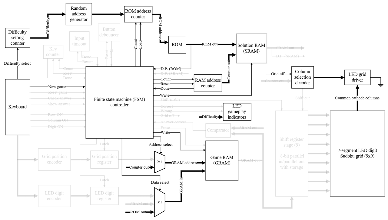
Input detected
When the system detects input, sequential user input (debounced) indicates to the FSM what type of data needs to be processed (row, column or digit values). Data is then encoded and saved to the appropriate registers. Once all inputs are processed (the key counter determines the type of data already processed) the Sudoku grid is temporarily turned off. A write cycle then takes in the user’s desired position, points the GRAM to this address, then writes in the requested digit at this grid location. Address counter and shift register stage are controlled to avoid losing the current grid position count before the write cycle. As mentioned, all 3 types of data must be detected within a certain timeframe, otherwise the system will reset to its natural state.
Grid initialization
For initializing the grid (once a new game starts) the difficulty must be determined. This is done independently from the FSM controller. Memory pages in ROM correspond to different difficulty levels. The FSM facilitates a ROM transfer to SRAM (solution RAM) for later solution checking, and to GRAM for printing the starting values of the Sudoku puzzle. The LED decimal point segments indicate the Sudoku grid starting values. The grid is turned off during the data initialization, and the “random” address generator is a free running counter cycling through a certain ROM page determined by user’s requested difficulty.
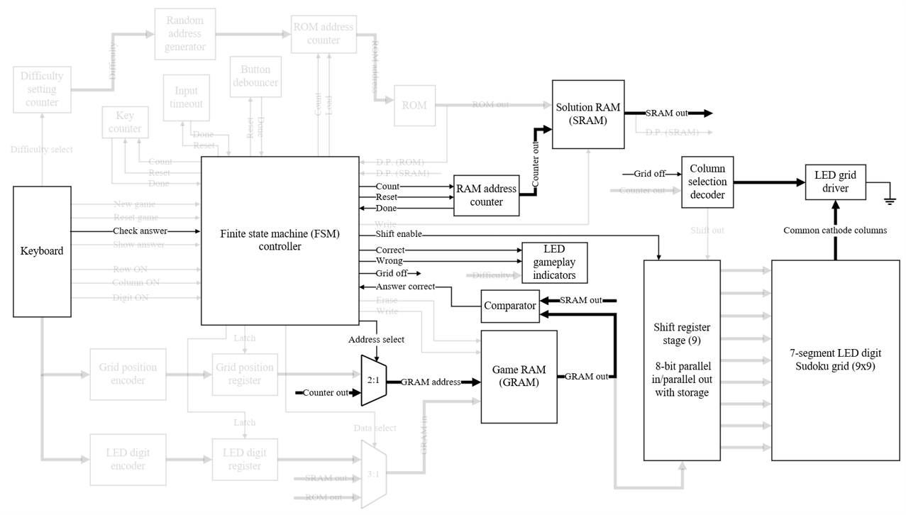
Solution checking
For checking the proposed solution, the grid is temporarily turned off. The RAM address counter cycles through the SRAM and GRAM addresses simultaneously, performing a byte-by-byte comparison. This indicates whether or not the correct solution was entered by the user (the decimal point segment is not considered). Once the RAM address counter reaches the last column/row position and the SRAM/GRAM comparison was identical throughout the whole grid, the solution is displayed as correct (by the green LED).
Reset game
The FSM starts a reset by erasing the GRAM data. Similarly to the ROM transfer, the LED decimal point segment indicates to the FSM whether or not the particular byte accessed is an initial value on the Sudoku grid. If it is, the SRAM data is used to rewrite the starting values to GRAM. The RAM address counter cycles through the SRAM and GRAM addresses simultaneously.
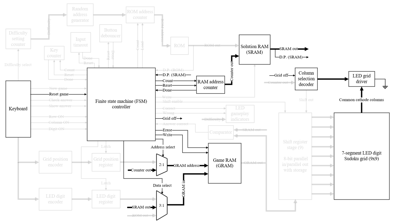
Give up and show solution
Finally, if the user gives up and wants to see the solution, the internal process is almost identical to the previous “Reset game” state, except that ALL of the SRAM data is printed to the GRAM (instead of only the starting values).
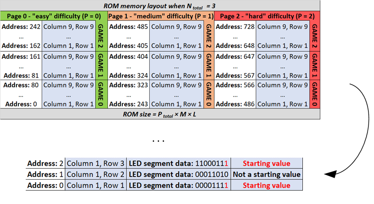
Solution storage
The actual Sudoku solutions are stored in ROM, which is divided into 3 memory pages. Each page corresponds to “easy” difficulty solutions, “medium”, then “hard”. In order to algorithmically determine where each game resides within each difficulty set, the following equations were derived.
L = size in bytes of a Sudoku game N = game index within a memory page/difficulty (zero index) P = page/difficulty Ntotal = total number of games for a given memory page/difficulty
The starting ROM address for a Sudoku game is L(N+PNtotal). Knowing this, the random address generator will count in increments of L(N+PNtotal) where N varies from 0 to (Ntotal - 1).
Once a new game is requested by the user, the ROM address counter will parallel load the current output of the random address generator.
Then, the ROM address counter will count from L(N+PNtotal) to L(N+PNtotal + 1) - 1.
Once the ROM address counter reaches L(N+PNtotal+1) - 1, it will notify the FSM with a DONE signal.
During ROM transfer if the least significant bit of the ROM data is HIGH (the LED decimal point segment), then this value is copied to GRAM.
Here’s an example of the memory layout using the above equations when the total number of games per difficulty is equal to 3.
Hardware schematics
The schematic for the design is broken into separate pages. At the heart of the system is a BeMicro MAX 10 FPGA dev kit. To connect the FPGA board to the rest of the system, an edge connector and jumper cables are used. 3 AA batteries are used as power.
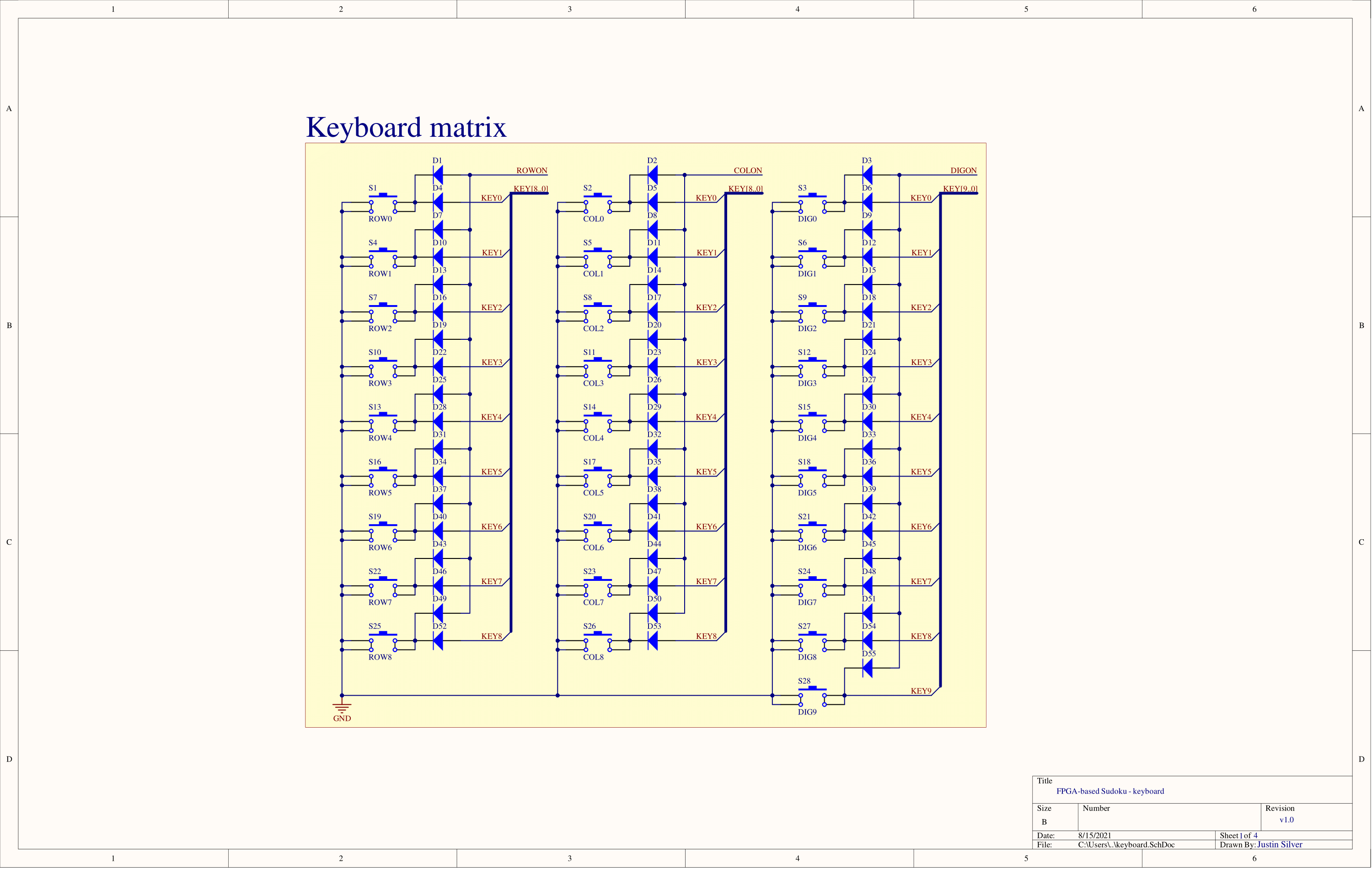
User input (keyboard multiplexing)
The keyboard contains 9 buttons for a row position, 9 buttons for a column position, and 10 buttons for inputting a digit (1-9 and CLEAR).
This multiplexed keyboard configuration results in a ROW_ON, COL_ON, or DIG_ON signal if a row, column, or digit button was pressed respectively (the input signals are connected to internal pullup resistors in the MAX10 FPGA). This lets the FSM to know what type of data it has to process.
The configuration employs blocking diodes that serve 2 different roles: one ensures that only a ROW_ON, COL_ON, or DIG_ON signal is active at a time, and the other ensures that only one bit on the KEY[9..0] bus is active
The 10th key bit corresponds to the CLEAR button and since this particular bit doesn’t share with any row or column buttons, only 1 diode is necessary.
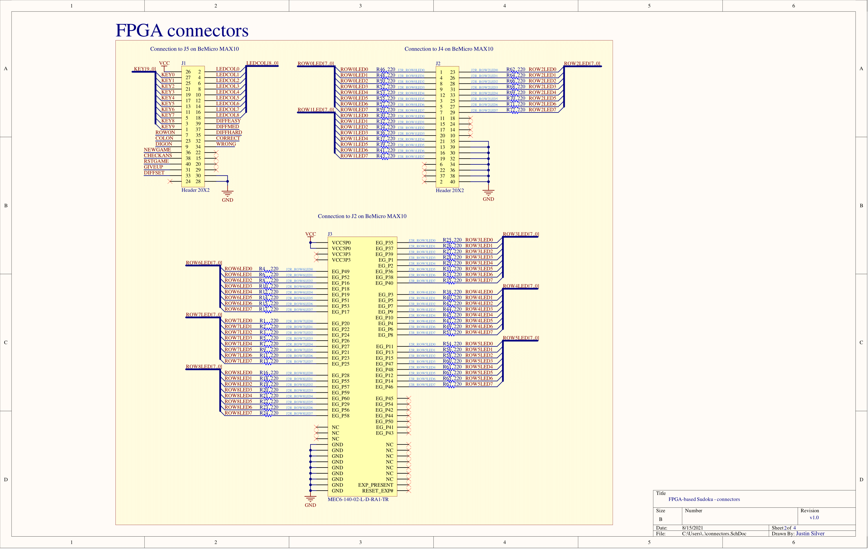
FPGA connections
The FPGA section of the schematic includes the various connectors that interface between the BeMicro MAX10 dev kit, and the I/O of the design.
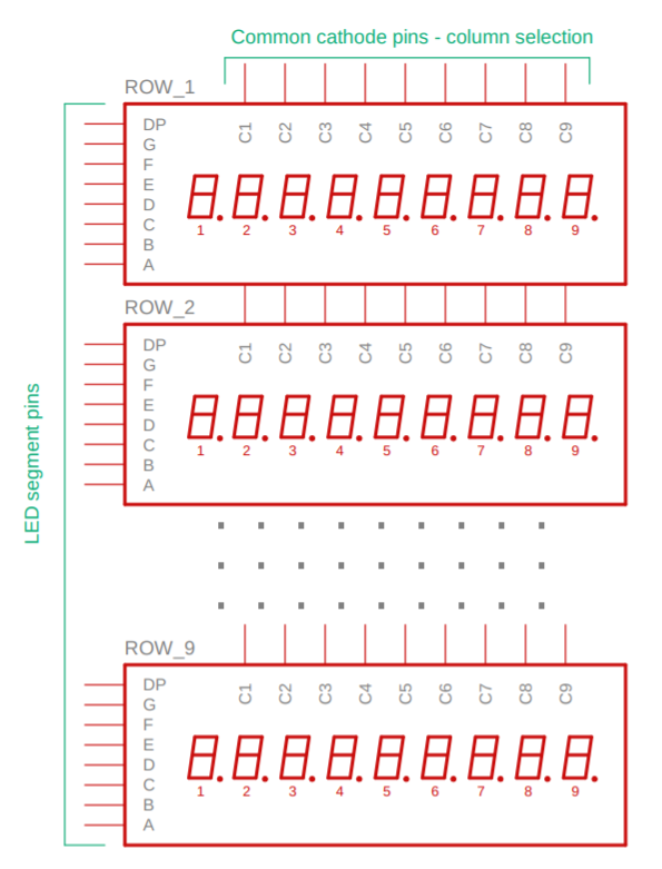
Sudoku grid display (LED multiplexing)
A combination of 27 7-segment LED displays gives a digit matrix of 9x9 (Sudoku grid!. One column of the grid is displayed at a time by setting the correspond column bit LOW (the displays are common cathode).
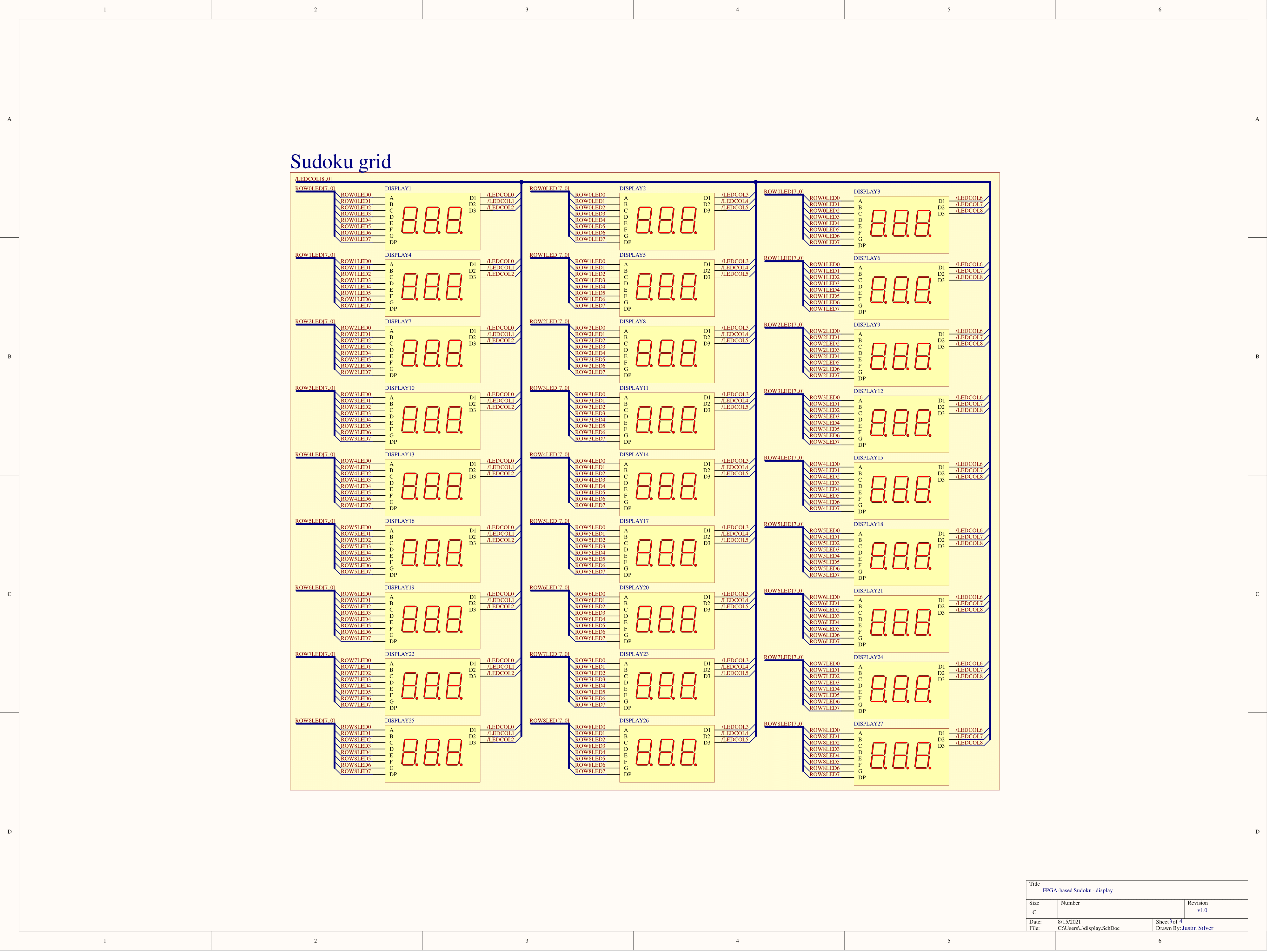
The following simplified diagram better illustrates the interconnections between the row and column nets.
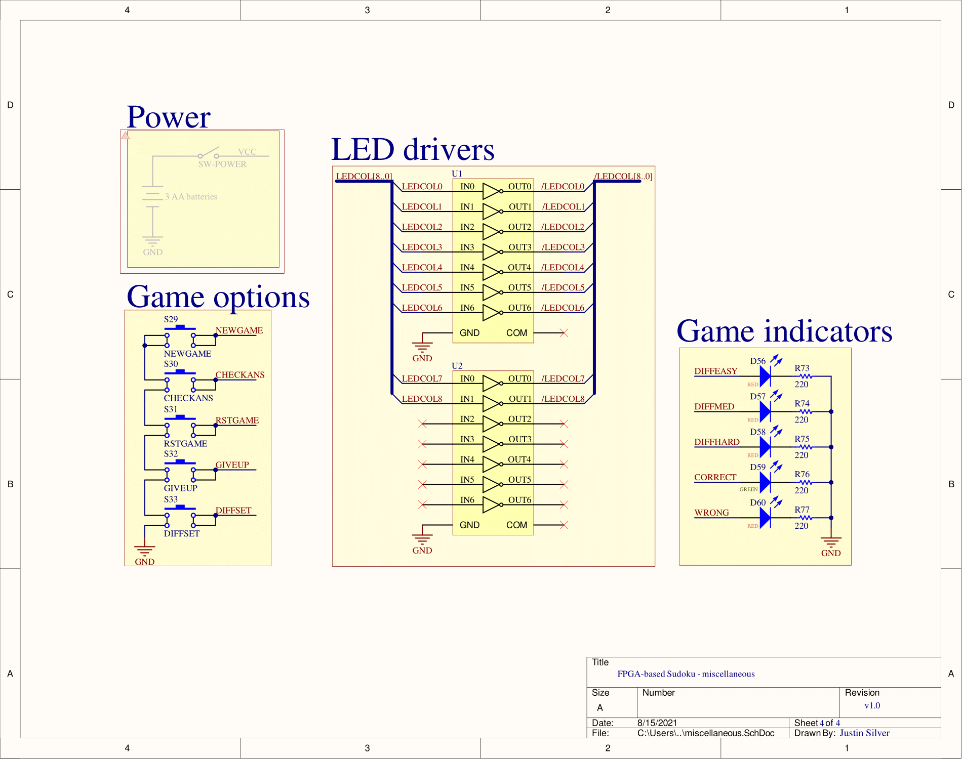
Miscellaneous
This portion of the schematic contains some other output indicators for the user (correct/wrong guess, difficulty level, etc.), the LED drivers for the grid, as well as other miscellaneous items.
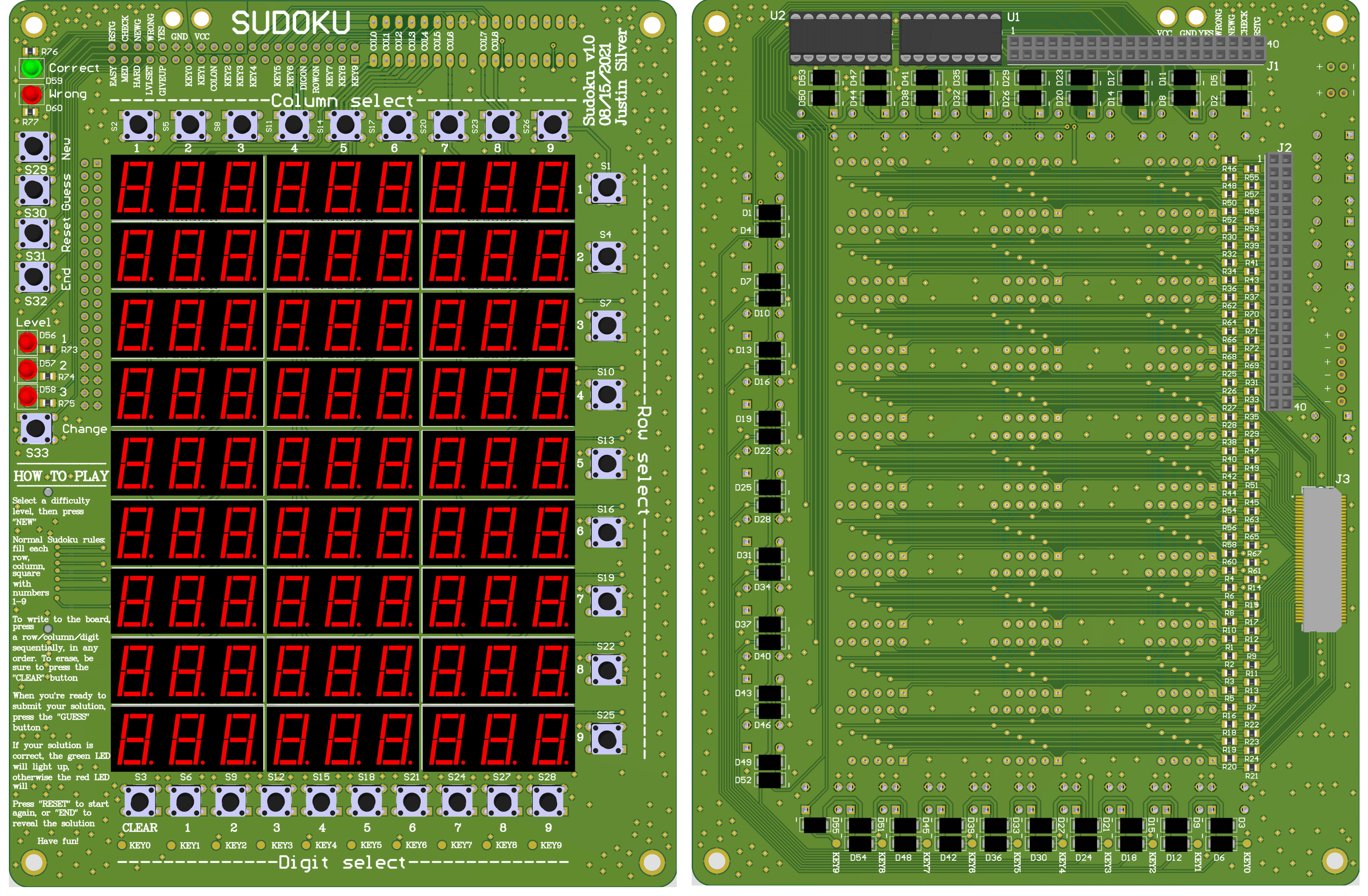
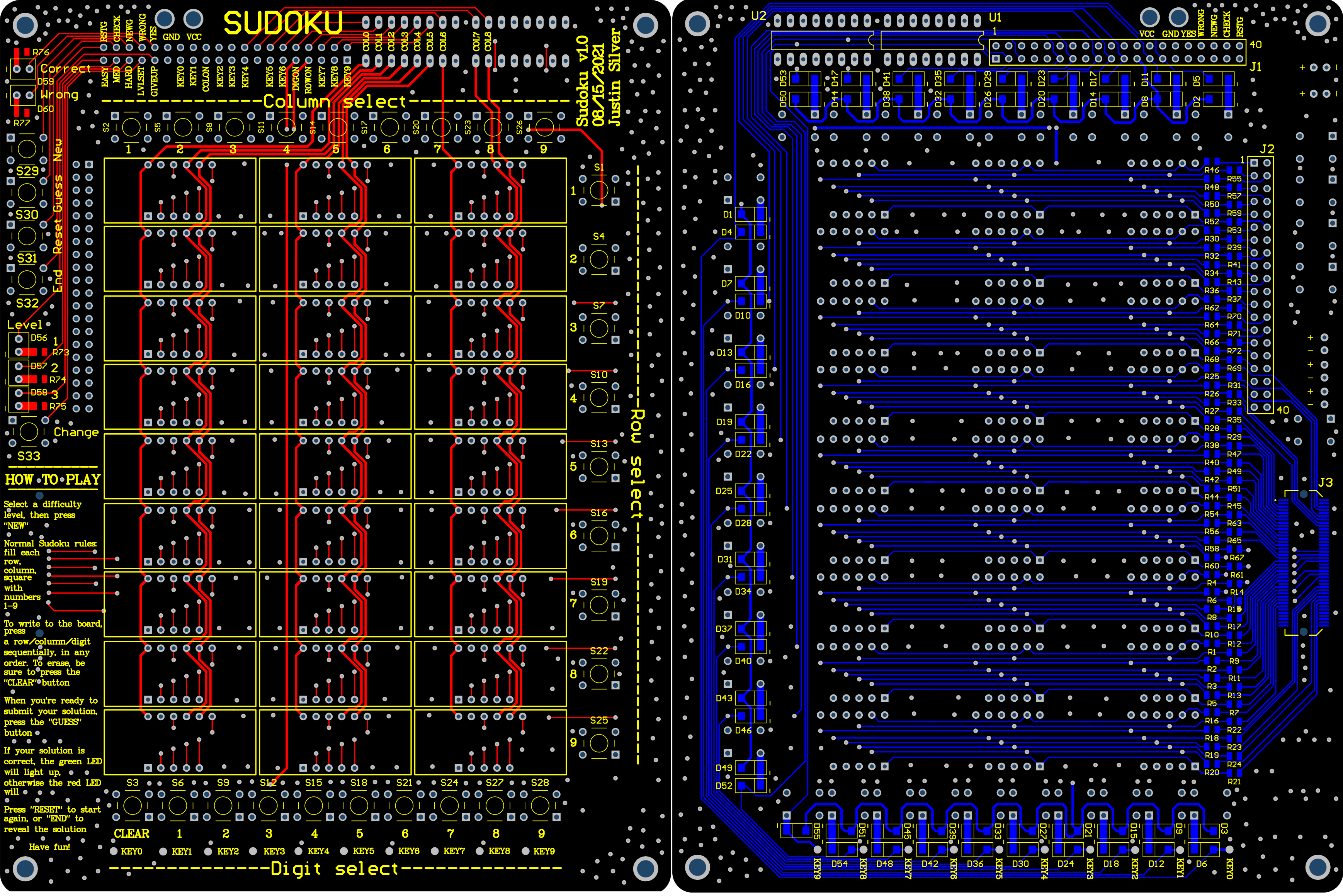
PCB design
The main constraints of the design were to reduce the size of the layout as much as possible, in order to achieve a similar form factor to that of a Sudoku booklet. As a result, there were many iterations on the component placement as well as pin locations for the various headers. The inputs/outputs associated with the board are low speed. The columns cycling only needs to beat persistence of vision, and all the inputs are tactile user buttons.
The board is a 2-layer stackup with ground pours, fabricated by JCLPCB. The top and bottom layers have copper GND pours, but to better visualize the traces, I’ve included images of the board without the pours.
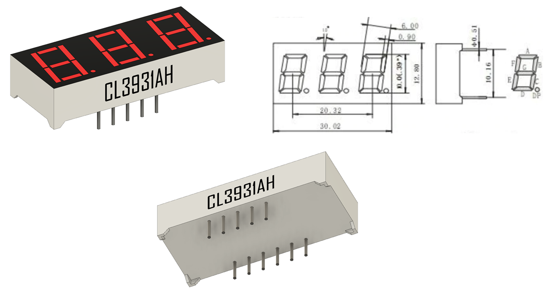
3D design of footprint
For use in visualizing the board, I created a simple Fusion 360 model for the LED modules. Dimensions of the model were taken from LED’s datasheet
Digital design
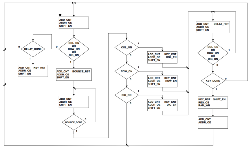
Finite State Machine ASM diagram
This FSM algorithm performs the following:
- Button debouncing
- Input timeout
- Processing user input
- Writes user input to GRAM
- Continually “prints” Sudoku grid
- Handles the access to GRAM by input registers and address counter
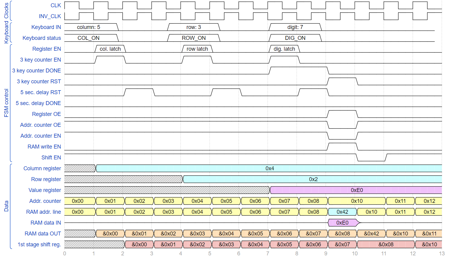
Chronogram – processing user input
Example chronogram: the number 7 at column 5, row 3 is written
- User presses 5th column button. At T1, FSM enables the column register to latch on to the encoded column position
- At T2, the 5 second timeout is reset
- At T4, another keyboard input is detected, but this time for the row position. The previous steps are repeated
- At T7, the process is repeated for latching in the encoded digit data
- The 3 key counter DONE signal tells the FSM to commence the write cycle
- At T9, the input registers take control of the RAM address/data lines for writing to the Sudoku grid
- At T10, a write operation is performed. Shift enable is set LOW and address counter paused to preserve row/column order after the write cycle
- At T11, the system returns to its initial state of cycling through the RAM’s addresses
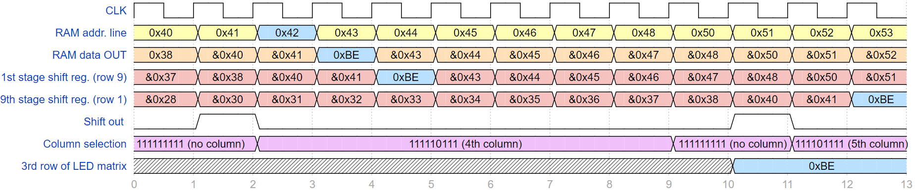
Chronogram – printing the Sudoku grid
- At T0, address 0x40 is set which corresponds to column 4, row 0.
- On the following rising edge of the clock, (T1) the memory contents at this address are available to be sent through the shift register stages.
- Note: it takes until T2 for the data to be latched into the first shift register stage. For this setup, the system is parallel shifting the data from the bottom up, or in other words, from row 9 to row 1.
- The address 0x42 (column 5, row 3) of the RAM holds the user data (0xE0) from the previous example (the digit 7).
- At T10, a “shift out” signal is enabled since the 1st stage shift register holds the segment data for the 5th column and 9th row, and the last stage shift register holds the data for the 5th column and 1st row (alignment)
- No column is selected immediately before and after enabling the shift out signal. This is done to avoid LED ghosting
Simulation
User input (keyboard multiplexing)
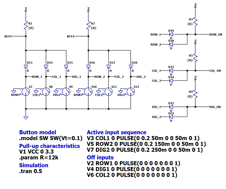
A LTspice simulation was constructed with a simplified keyboard (6 buttons - 2 column buttons, 2 row buttons, and 2 digit buttons) that has the same diode configuration as the hardware schematic. The pull-up resistors represent the internal resistors of the FPGA. Contact bouncing was ignored for simplicity.
The sequence to test: User inputs 1st column, 2nd row, and 2nd digit.
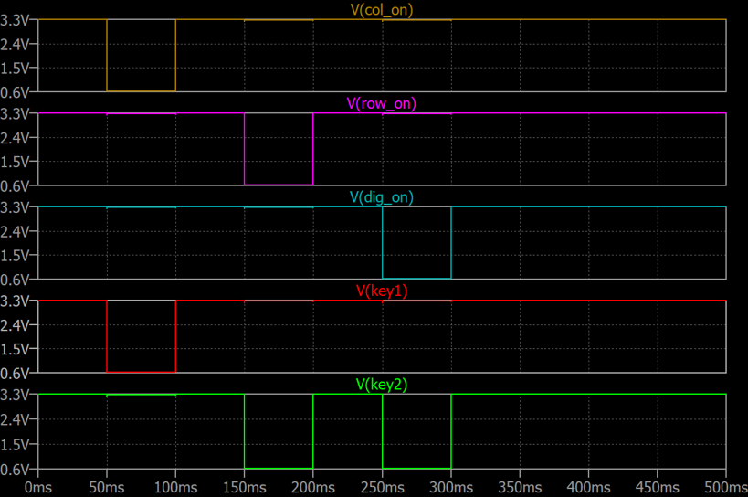
The simulation results show that the “ON” signal for the various data inputs as well as the appropriate KEY bit can be determined.
- T = 50 ms, 1st column is pressed
- T = 150 ms, 2nd row is pressed
- T = 250 ms, 2nd digit is pressed
Sudoku grid display (LED grid driving)
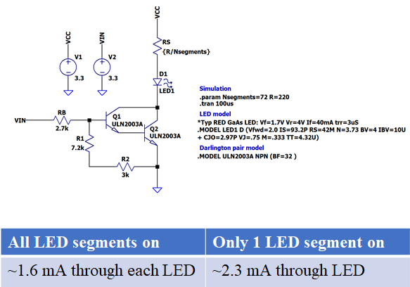
Another simulation was built for determining the current through the LED grid segments. A Darlington pair (IC ULN2003A) was used for high current gain (since there is a potential to drive 72 LED segments in parallel). For the highest current gain, it is necessary to put the transistors in their active mode (ensure that VCE > VCE(sat) for the Darlington pair transistors)
Identical current branches placed in parallel (i.e. the number of LED segments ON within a column) are treated as a varying collector resistor. For example, if 2 LED segments are ON then the collector resistance value is divided by 2.
The series resistance (RS) was chosen for the worst case scenario: if VCE = 0, then IC < 6 mA (current limiting)
It was difficult to assure linear mode because RS changes with increasing number of segments that are turned on.
To have a maximum current with the imposed constraints, VIN and VCC is set to 3.3 V (FPGA limits)
BJTs are in/close to saturation, but LTspice indicates at least 1.6 mA per segment branch.
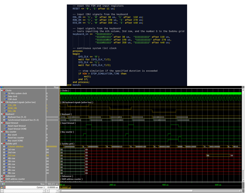
Simulation/testbench - ModelSim
This simple testbench simulates a user performing the following input sequence: 6th column, 3rd row, and the digit “5”
Proof of concept hardware test
To test the system architecture, a proof of concept breadboard test with a reduced keyboard and LED matrix was performed. The particular test only targets processing user keyboard input and continual printing to the Sudoku grid. The LED digit modules were arranged as 2 rows, 3 columns
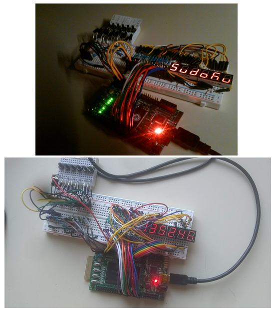
This short video shows how a sequential user input leads to a Sudoku grid update.
Summary, conclusions
What I learned
Because this project incorporated so many different aspects of electrical engineering, I made a list of the various concepts that I got experience with.
Digital design
- FPGA development (VHDL, testbenches, simulation, vendor software packages)
- Digital logic (counters, encoders, bus multiplexers, RAM/ROM, etc.)
- Finite state machine design with datapath
- Timing diagrams (chronograms)
- Basic TCL scripting
Analog design
- PLL basics
- Keyboard/LED multiplexing (blocking diodes)
- LED driver (Darlington pair)
- LTspice circuit simulation
Hardware/system design
- Altium designer for schematics and PCB design
- Microsoft Visio for block diagrams
- Wavedron for chronograms
- GIMP for image design
- Fusion 360 for 3D PCB components
Other
- Git and GitHub for version control
- Documentation (personal website)
- Budgeting and buying components
- Datasheets
- Debugging
Obstacles, challenges
Of course, the project wasn’t without its challenges:
- Learning and navigating through software/CAD tools (Quartus II, Altium, Visio, etc.)
- Resource limitations
- Implementation of a FSM controller
- Synchronous clock domain crossing
- Debugging hardware
- Button debouncing
- Clear and concise block diagrams
- Version control
- Budgeting my time (school, internship)
- Feature creep
Future work
Finally, the following is a non-exhaustive list of the work left to be done:
- Finish PCB layout
- Fabricate PCB at my university or FabLab (routing/clearance restraints)
- Component buying
- Soldering all components onto PCB
- Hardware test
- Updating FSM to perform all functionalities previously discussed
- Designing new functional blocks (ROM, ROM counter, comparator, etc.)
- 3D printing of an enclosure for the device
- Continuing documentation on website